
Quantum Electron Device Research Team
Principal Investigator
| PI Name | Michihisa Yamamoto | ||||||||||||
|---|---|---|---|---|---|---|---|---|---|---|---|---|---|
| Degree | D.Sci. | ||||||||||||
| Title | Team Leader | ||||||||||||
| Brief Resume |
|||||||||||||
|
|||||||||||||
Outline
We develop quantum electron devices based on manipulation and transfer of quantum degrees of freedom in solids. We employ quantum electron optics, where quantum states of propagating electrons are manipulated in a single electron unit, and experiments on transfer and manipulation of novel quantum degrees of freedom in atomic-layer materials. These experiments aim to reveal physics of quantum coherence, quantum correlations, and quantum conversions, as guiding principles for quantum electron devices. We also employ state of the art quantum technologies to solve long-standing problems in condensed matter physics from microscopic points of view.
Research Fields
Physics, Engineering
Keywords
Two-dimensional electron systems
Single electron manipulation
Nanodevices
Quantum coherence
Quantum correlations
Results
Observation and control of the Kondo screening cloud
The Kondo effect, an archetype of many-body correlations, arises from the interaction between a localized spin and surrounding conducting electrons. Since conducting electrons form a spin cloud to screen the localized spin, the Kondo state is also called as the Kondo cloud. The size of the Kondo cloud is one of the most important parameters that determine properties of many-body states containing multiple localized spins.
We confined a localized spin in a semiconductor artificial atom coupled to conducting electrons, embedded it into an electronic interferometer, and observed real shape of the Kondo cloud. We found that its size is inverse proportional to the Kondo temperature and that the cloud has the universal shape. More recently, we also found that the spin screening state can be electrically controlled.
Our work is an important step towards understanding of many-body correlated states containing multiple magnetic impurities and development of novel quantum information devices based on the long-range spin coupling. We are now investigating systems, where multiple Kondo clouds overlap with one another.
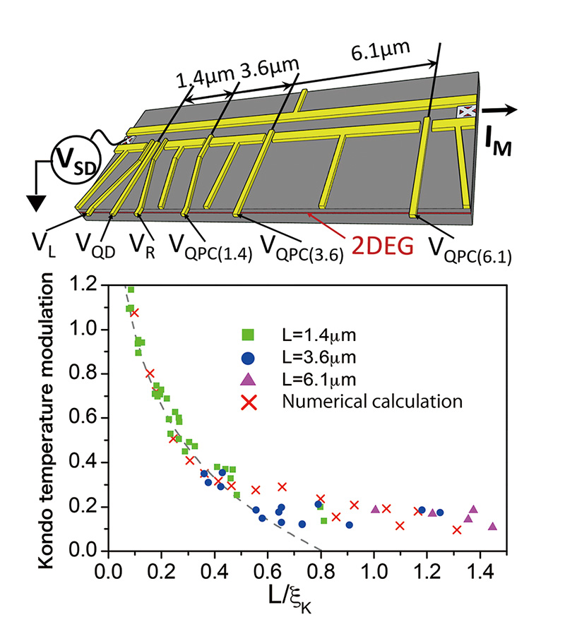
Schematic illustration of the device used for detection of the Kondo cloud and real shape of the Kondo cloud. The Kondo cloud shape was obtained by quantifying the Kondo temperature modulation by the gate voltage VQPC applied to the quantum point contacts.
Figure taken from Nature 579, 210 (2020).
Quantum control of electron waves and measurement of the scattering phase
The phase of an electron wave function, a counterpart of the wave function amplitude characterizing the electron probability density, plays an important role in quantum devices. Techniques for precise measurement and control of the phase shift of an electron wave are useful not only for development of quantum devices but also for investigation of microscopic quantum effects in solids that cannot be detected in conventional transport experiments. We employ quantum electron optics, where the quantum state of a propagating electron is manipulated, to investigate scattering of an electron wave by an artificial atom.
We recently apply this technology for quantum control of electron waves to the quantum information processing. Based on the electron wave states, we attempt to control delocalized quantum bits defined by on-demand special quasi-particles. Similarly to the photon qubit, where the number of qubits is not limited by the hardware size, this may open up a way to control numerous semiconductor qubits in a compact hardware. Our aim is to bring a paradigm shift in semiconductor quantum architectures, from vast infrastructure to a much smaller hardware, by realizing quantum control of on-demand qubits.
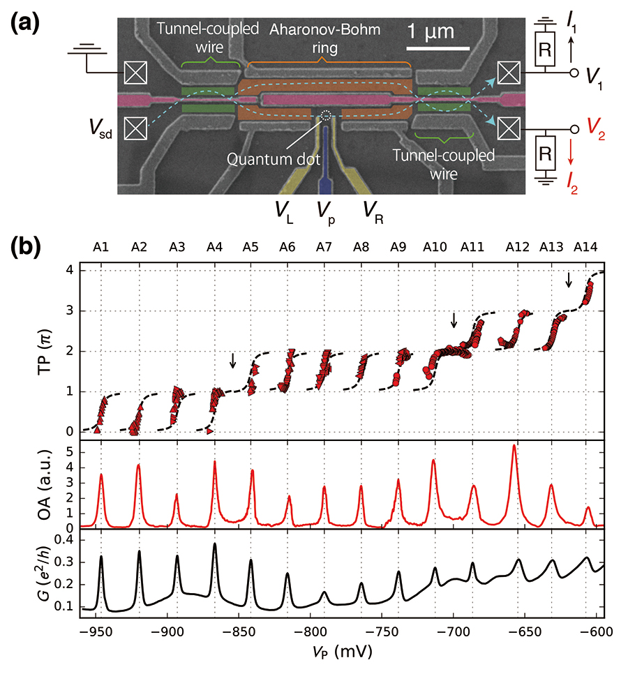
(a) Scanning electron micrograph of the device and experimental setup for the phase measurement across an artificial atom. Output currents I1 andI2 oscillate with opposite phase as a function of the difference of phase shift acquired in the two paths of the Aharonov-Bohm ring. (b) Phase shift through a quantum dot extracted from the oscillating component of the measured current I = I1 – I2, plotted with the oscillation amplitude and the total conductance. Phase lapse appears between Coulomb peaks (maximum of the conductance through the quantum dot), depending on the parity of orbital wave function in the quantum dot.
Figure (b) taken from Nature Communications 8, 1710 (2017).
Members
Michihisa Yamamoto |
Team Leader | michihisa.yamamoto[at]riken.jp | |
|---|---|---|---|
Yuya Shimazaki |
Research Scientist | ||
Han Ngoc Tu |
Postdoctoral Researcher | ||
David Pomaranski |
Visiting Scientist |
Publications
- M. Tanaka, K. Watanabe, T. Taniguchi, K. Nomura, S. Tarucha, and M. Yamamoto
Phys. Rev. B 105, 075427 (2022)Temperature-induced phase transitions in the correlated quantum Hall state of bilayer graphene
- R. Ito, S. Takada, A. Ludwig, A. D. Wieck, S. Tarucha, and M. Yamamoto
Phys. Rev. Lett. 126, 070501 (2021)Coherent beam splitting of flying electrons driven by a surface acoustic wave
- M. Tanaka, Y. Shimazaki, I. V. Borzenets, K. Watanabe, T. Taniguchi, S. Tarucha, and M. Yamamoto
Phys. Rev. Lett. 126, 016801 (2021)Charge Neutral Current Generation in a Spontaneous Quantum Hall Antiferromagnet
- I. Borzenets, J. Shim, J. C. H. Chen, A. Ludwig, A. D. Wieck, S. Tarucha, H. S. Sim, and M. Yamamoto
Nature 579, 210 (2020)Observation of the Kondo screening cloud
- Y. Shimazaki, M. Yamamoto, I. V. Borzenets, K. Watanabe, T. Taniguchi, and S. Tarucha
Nat. Phys. 11, 1032 (2015)Generation and detection of pure valley current by electrically induced Berry curvature in bilayer graphene
2-1 Hirosawa, Wako, Saitama 351-0198 Japan
E-mail:
michihisa.yamamoto[at]riken.jp