We work on the development of new organic semiconducting polymer materials and their application to organic electronic devices. Specifically, relying on the basic chemistry of the intermolecular interactions during the film forming process from the solutions, we seek the methodology and the molecular design to control the precise structures in molecular- and nano-scale at our will, and try to find breakthroughs to drastically enhance the performance of the organic electronic devices. Targets of our research are not only the conventional organic solar cells and field-effect transistors, but also the organic electronic devices with new functions based on the structure controls.
Unveiling the Cause of Performance Variations in Organic Semiconductor Polymers for Solar Cells
Organic thin-film solar cells have attracted attention as next-generation energy sources due to their lightweight and flexible properties. However, a significant challenge lies in the performance variation of the semiconductor polymers used in these solar cells, which occurs between different synthesis batches. This variation is generally attributed to differences in molecular weight distribution, but this factor alone cannot fully explain the observed performance inconsistencies. In particular, the high-performance semiconductor polymer PM6 is composed of two alternating units, BDT and BDD. During synthesis, structural defects such as “-A-B-B-A-B-” may occur instead of the ideal alternating structure “-A-B-A-B-“. Such structural defects are believed to contribute to performance variations, yet methods for their quantitative evaluation have been limited.
In this study, we developed a novel method using X-ray photoelectron spectroscopy (XPS) to precisely evaluate the main chain structure of semiconductor polymers. By employing Y6 and BTP-eC9 as standard samples, we accurately calculated the relative sensitivity factor (RSF), enabling the unit ratio in PM6 to be assessed with a precision of approximately 1%. Evaluation of three commercial PM6 samples revealed that all samples exhibited an excess of BDD units, with the degree of excess varying between suppliers. This structural deviation correlated with variations in solar cell performance. These findings provide valuable insights for semiconductor polymer quality control and material design, contributing to the stable production of high-efficiency organic thin-film solar cells.
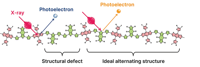
Main Chain Structure Repetition and Structural Defects in Semiconductor Polymer PM6
Organic Semiconductors Exhibiting Intramolecular Double Proton Transfer
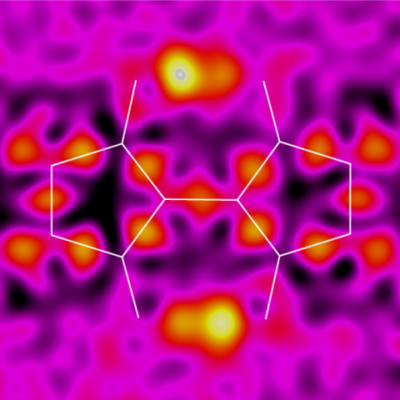
To investigate potential applications of the 3,3′-dihydroxy-2,2′-biindan-1,1′-dione (BIT) structure as an organic semiconductor with intramolecular hydrogen bonds, a new synthetic route under mild conditions is developed based on the addition reaction of 1,3-dione to ninhydrin and the subsequent hydrogenation of the hydroxyl group. This route affords several new BIT derivatives, including asymmetrically substituted structures that are difficult to access by conventional high-temperature synthesis. The BIT derivatives exhibit rapid tautomerization by intramolecular double proton transfer in solution. The tautomerizations are also observed in the solid state by variable temperature measurements of X-ray diffractometry and magic angle spinning 13C solid-state NMR. Possible interplay between the double proton transfer and the charge transport is suggested by quantum chemical calculations. The monoalkylated BIT derivative with a lamellar packing structure suitable for lateral charge transport in films shows a hole mobility of up to 0.012 cm2 V−1 s−1 with a weak temperature dependence in an organic field effect transistor.

Electron density difference analysis of X-ray structure analysis has observed protons exchanging between two positions in the center of the molecule.
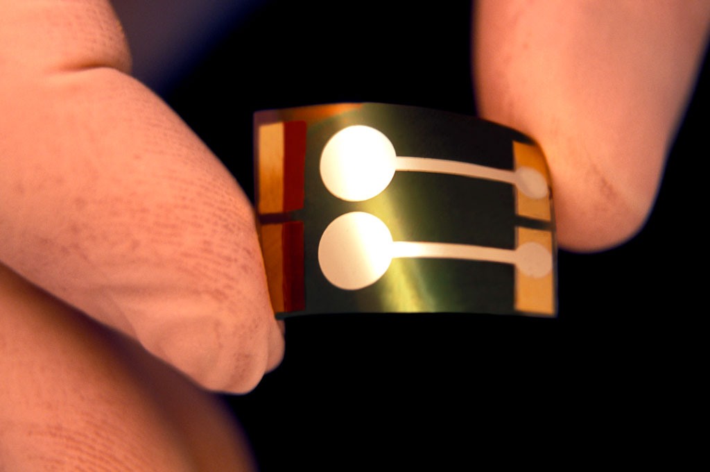
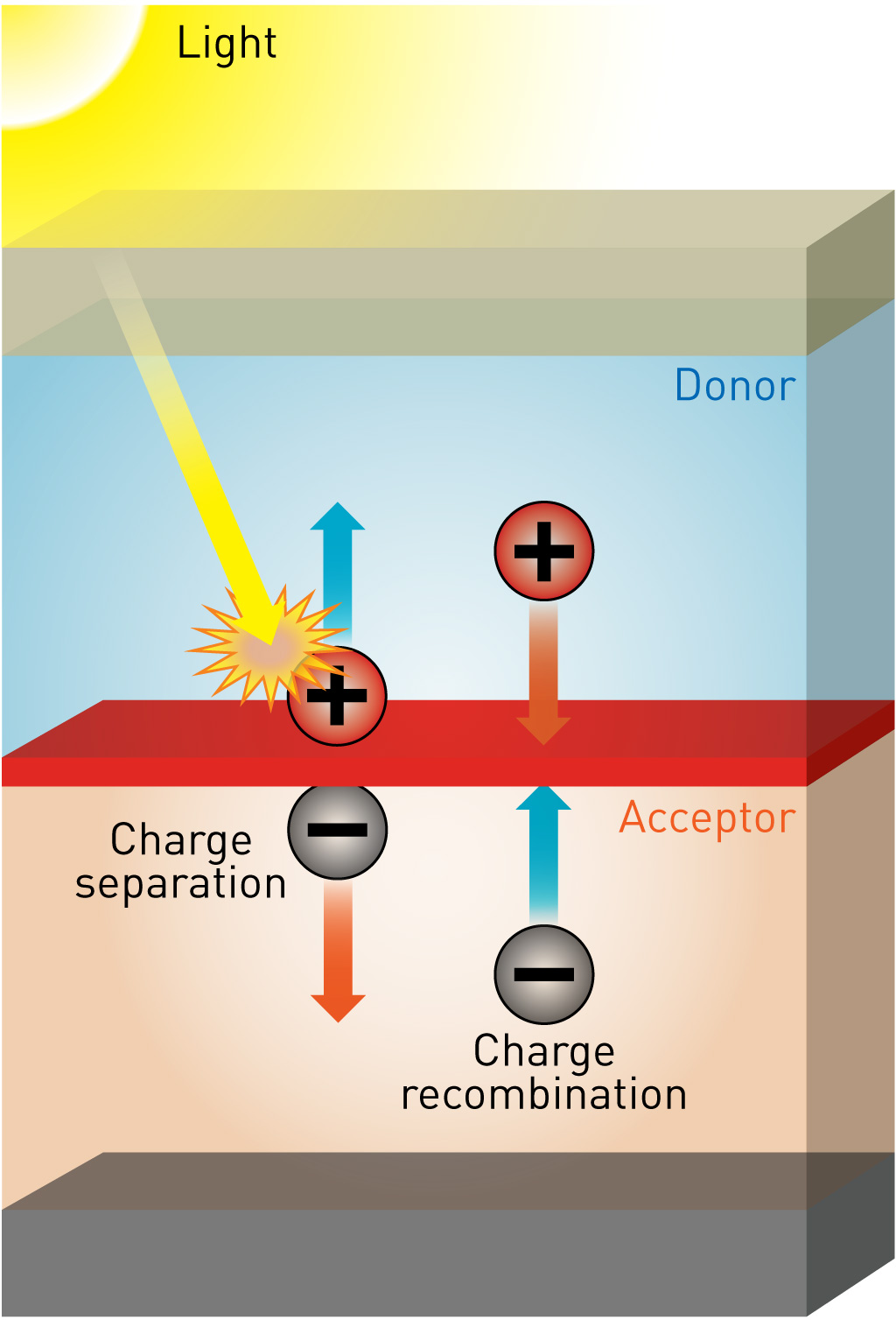
Energetic driving force for charge generation in organic solar cells
For further improvement of the device performance of organic solar cells, optimization of electron-donating material and electron-accepting material is necessary. However, we first need to know the most suitable electronic structures for these materials. The problem was the lack of knowledge on the relation between the energetic driving force at the donor and acceptor interface and resulting device performance. To investigate the relationship between the interfacial energetic driving force and resulting device performance, the planar-heterojunction structures with simple and well-defined interfaces of electron-donating material (D) and electron-accepting material (A) are investigated. 16 planar-heterojunctions with four donor materials and four acceptor material were systematically investigated. We found that for efficient charge generation, molecularly excited state (S1) and interfacial charge-transfer (CT) state must have an energetic difference of 0.2~0.3 eV. This result provides a valuable guideline for the molecular design for efficient organic solar cells.

The charge generation efficiency is plotted against the energetic difference between the singlet excited state and charge-transfer state.
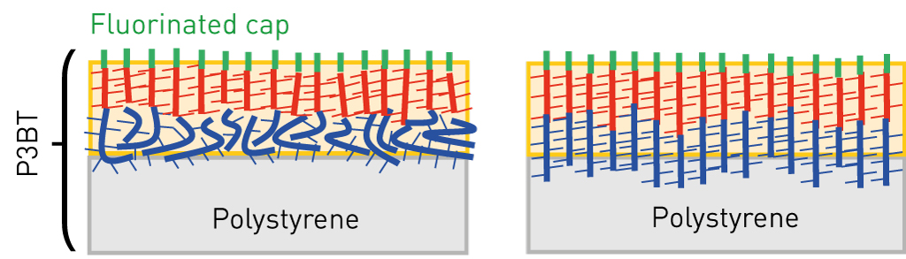
Crystallization of organic semiconductor in thin film induced from surface
Highly ordered crystalline thin films are required for organic electronics devices such as organic field effect transistors and organic photovoltaics. Rather complicated dynamic approaches have been reported to obtain large crystalline domains in solution-processed films. The interactions between the molecules and the substrate surface also play an important role in controlling the crystal structures and their orientation in thin films, known as template (or epitaxial) growth, but its application is mostly limited to evaporated films.
We discovered that self-assembled surface segregated monolayers can induce the crystallization of organic semiconducting materials in thin film from the surface. An unprecedentedly highly crystalline film of a methanofullerene derivative is formed simply by heating the film after spin-coating. The crystal structure induced by the surface was completely different from the known structure for the compound and oriented in the direction of the film normal. Owning to the high crystallinity, the electron mobility in the vertical direction was about five times higher than in the ordinally multicrystalline films. This new concept paves the way for enhancing the performance in various organic electronic devices.

(left) X-ray diffraction pattern of the fullerene derivative in thin films after crystallized from the surface and (right) the crystal packing structure obtained from the pattern.
Reproduced with permission. Copyright 2018, Wiely-VCH. DOI: 10.1002/anie.201801173