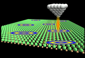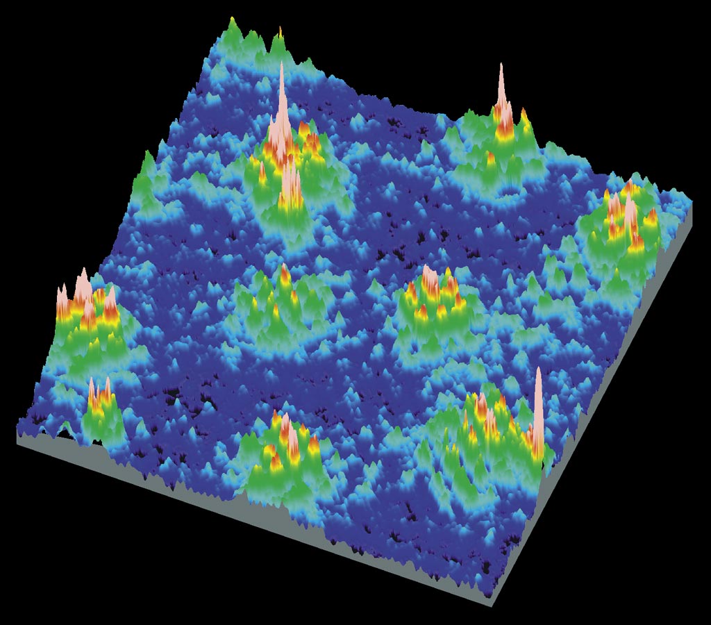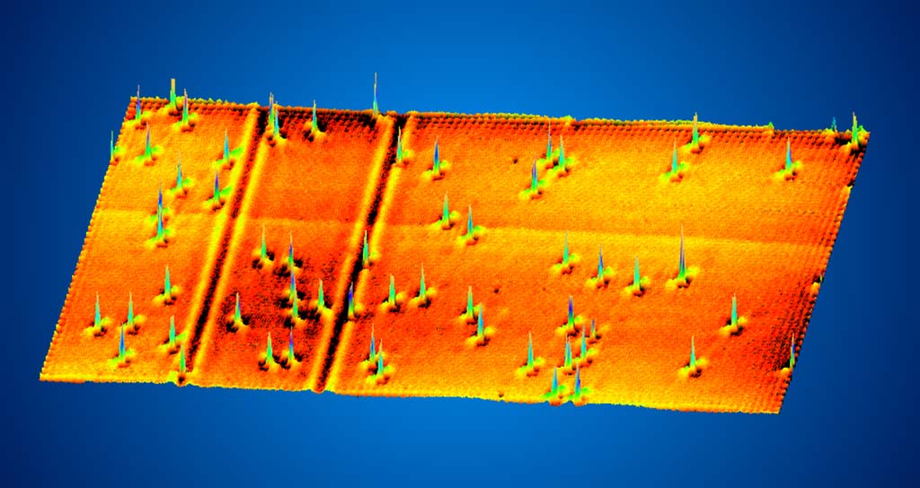
We experimentally study electronic states related to emergent phenomena in electron systems, such as high-temperature superconductivity and topological quantum phenomena. For this purpose, we use scanning tunneling microscopes working under combined extreme conditions of very low temperatures, high magnetic fields and ultra-high vacuum. Modern scanning-tunneling-microscopy technology enables us to obtain a “map of the electronic state” with atomic-scale spatial resolution. We make and analyze the maps of various materials and establish the relationships between material properties and electronic states. We also pursue the development of novel measurement techniques to discover new emergent phenomena in condensed matter.
Direct imaging of massless electrons at the surface of a topological insulator
Topological insulators are a new phase of matter which was discovered recently. Although it is an insulator in the bulk, a topological insulator possesses a metallic surface where electrons lose their mass. The surface state is expected to serve as a base of spintronics application, because spins of massless electrons can be used to handle information. However, the experimental understanding of massless electrons is still elusive.
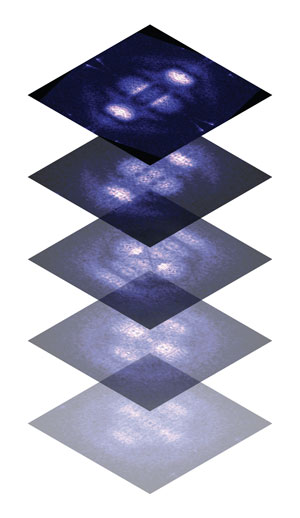
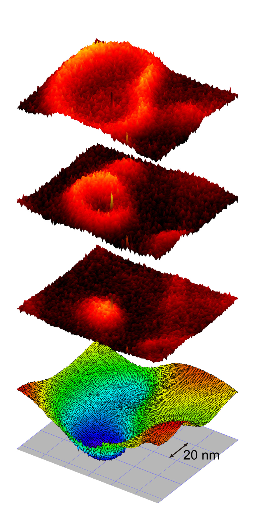
Using scanning tunneling microscope, our team succeeded in imaging the nano-scale spatial structure of massless electrons at the surface of a topological insulator Bi2Se3. We focus on imaging in a magnetic field, where electrons exhibit cyclotron motion. The center of the cyclotron motion drifts around the charged defect, resulting in an “electron ring”. We found that the unique character of massless electrons manifests itself in the internal structure of the electron ring. The observed internal structure is related to the spin distribution and will give us an important clue for future spintronics applications.

“Electron rings” at different energies.


