Semiconductor Science Research Support Team
Principal Investigator
- PI Name
- Fumihiro Matsukura
- Degree
- D.Sci.
- Title
- Team Director
- Brief Resume
1994 Research Associate, RIEC, Tohoku University 2006 Associate Professor, RIEC, Tohoku University 2012 Professor, AIMR, Tohoku University 2018 Professor, CIES, Tohoku University 2023 Team Leader, Semiconductor Science Research Support Team, RIKEN Center for Emergent Matter Science (-present)
Position name has been changed to Team Director as of April 1, 2025
Outline
Our mission is to develop novel technologies in nanoscience and nanotechnology and to support the users in RIKEN for the fabrication and characterization of nanoscale devices. We are responsible for the operation of the facilities including the cleanroom (ISO class 5) and the chemical rooms with suitable safety measures by educating the users.
Research Fields
Physics, Materials Science
Keywords
Nanometer-scale fabrication
Sample characterization
Education of users
Results
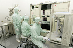
Supporting nano-device fabrication
To build a sustainable society, it is essential to realize devices with low power consumption and high-speed operation based on nanotechnologies. In Center for Emergent Matter Science, researchers are developing quantum and spin devices by using state-of-the-art equipment with its best condition Our team is established to support the researcher’s activity by providing skillful expertise. We are responsible for the operation of equipment like lithography systems including electron-beam lithography systems, maskless UV photolithography systems, deposition systems like evaporators and sputters, dry and wet etching systems and observation system like scanning electron microscopy. We instruct users in the usage of equipment and provide technical information in fabrication. With our effort, the researchers are now able to fabricate and characterize various devices in the range of 10 nm – 10 µm routinely.

Devices fabricated in the cleanroom.
Members
Fumihiro Matsukura |
Team Director | fumihiro.matsukura[at]riken.jp | |
|---|---|---|---|
Reiko Nakatomi |
Technical Staff I | ||
Yoshio Taguchi |
Technical Staff I | ||
Hideaki Oyama |
Technical Staff I |
Contact Us
Nanoscience Joint Laboratory,
2-1 Hirosawa, Wako, Saitama 351-0198 Japan
E-mail:
fumihiro.matsukura
[at]riken.jp