The purpose of our group is to discover novel properties and create revolutionary functions, based on nanodevices of two-dimensional (2D) materials, 1D nanotubes, and 0D quantum dots (QD) as well as topological materials. Our focus is superconductivity, phase transitions, and nonreciprocal transport, using 2D materials and their van der Waals heterostructures, and a wide range of carrier density tuning using electric double layer transistors. We also develop several novel solution-processable QDs, assemble them into various arrangements, and realize various functionalities including thermoelectricity, photovoltaics, and charge storage.
Bulk photovoltaic effect induced by symmetry control of two-dimensional materials
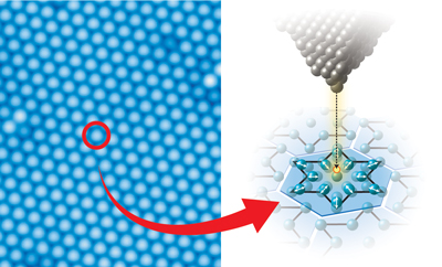
Our group is studying nonreciprocal transport in semiconductors and superconductors. One of them is a bulk photovoltaic effect, where the photoelectric conversion occurs without PN junctions. Monolayer transition metal dichalcogenides (TMDs) are two-dimensional materials with three-fold symmetry, which are known not to exhibit bulk photovoltaics. However, such a nanomaterial is capable of changing symmetry either by deforming or creating heterojunctions. This is a unique and important feature of nanomaterials that distinguishes them from bulk. Specifically, we have found strong bulk photovoltaic effects in the visible to infrared region in WS2 nanotubes, WSe2/black phosphorus van Waals heterojunctions, and strained MoS2 (Refs. Nature 570, 349 (2019), 3, 5). We found that the shift current mechanism plays an important role in this photovoltaic effect. Symmetry-controlled nanomaterials showing such large photovoltaic effects will be a promising new platform for high-efficiency photovoltaics and sensors.
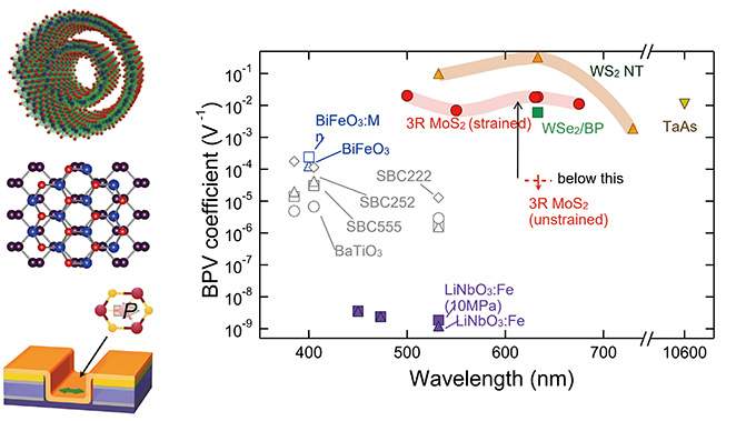
Left: Symmetry controlled TMDs. From the top, TMD nanotube, van der Waals heterostructure, and strained device. Right: Wave length dependence of bulk photovoltaic coefficient for nano TMDs.
Copyright: Left: Adapted from “Nature Nanotechnology 18, 36 (2023).”
Quantum materials and their nanodevices toward revolutionary physical properties and energy functions
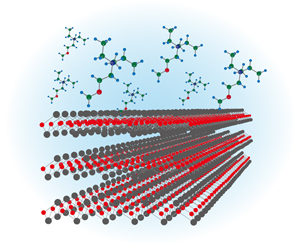
FeSe is a unique 2D superconductor, where the critical temperature exhibits a dramatic jump from 8 K to 40 K by reducing the thickness from bulk to monolayer. However, due to the difficulty in fabrications, the transport properties has remained elusive. We fabricated FeSe monolayer films by means of an iontronic technique, and succeeded in the first measurement of thermoelectric properties.
Left figure shows an electric double layer transistor (EDLT) device of a FeSe monolayer. FeSe monolayer was obtained through the detailed control of electrochemical etching processes with temperature and gate voltages. Right figure summarizes the temperature dependence of thermoelectric power factor P for various materials including monolayer FeSe. We found that monolayer FeSe exhibits gigantic value of 250 μW/cm/K2 beyond that of well-known thermoelectric material Bi2Te3. Furthermore at low temperatures, record-high P values are observed exceeding all reported materials. This example unambiguously demonstrates that 2D and related materials are highly promising for our purposes.
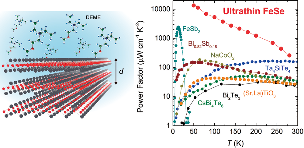
Left: Monolayer FeSe device fabricated by an iontronic technique
Adapted from “Nature Communications 10, 825 (2019).”
Right: Temperature dependence of thermoelectric power factor of monolayer FeSe and other materials
Iontronics toward Revolutionary Energy Materials
We are proposing a new concept “iontronics”, which means electronics controlled by motions and arrangements of ions. By introducing Iontronics, we are nowadays able to go beyond the conventional current switching devices and to realize voltage-controlled electronic phase transitions, including superconductivity, ferromagnetism, and metal-insulator transitions. Iontronics is growing up to an interdisciplinary field stemming from electrochemistry, materials science, condensed matter physics to energy materials.
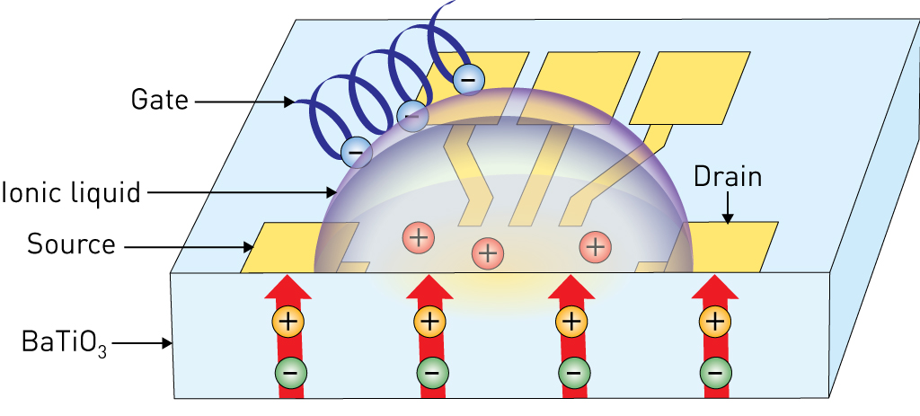
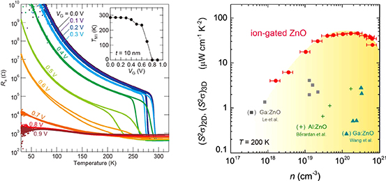
A representative device iontronics is an electric double layer transistor (EDLT), which enables the high density carrier accumulation at the electrolyte-solid interfaces. Left figure shows the temperature-dependence of resistance of vanadium dioxide (VO2), demonstrating the field-induced insulator-metal transition with only 1 V. Right figure depicts the optimization of the thermoelectric power factor in zinc oxide (ZnO), an archetypal oxide semiconductor, as a function of carrier density, demonstrating a comparable power factor to that of the practically used Bi2Te3. These achievements are indicating novel routes toward the next generation low power consumption devices as well as revolutionary energy materials.
Left: Gate-induced esistance switching in VO2 EDLT.
Adapted from “Nature 487, 459-462 (2012).” with permission (© 2012 Nature)
Right: Optimization of thermoelectric power factor of ZnO with EDLT.
Adapted from “PNAS, 113, 6438-6443 (2016).” with permission